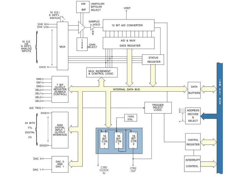
● PCI Bus
● Type: Successive approximation.
● Resolution:12-bit
● Conversion Time: 8 μsec max., 5.7 μsec typical.
● Integral Linearity Error: ±0.45 LSB maximum.
● Differential Non-Linearity: No missing codes.
● Monotonicity: Guaranteed over operating temperature range.
● Linearity: ±1 bit.
● Zero Drift: ±10 ppm/°C maximum.
● Gain Drift: ±45 ppm/°C maximum.
● Trigger Source: Software selectable, external trigger, programmable timer, or program command.
● Acquisition Time: 1 microsecond to 0.01% typical for full scale step function input.
● Aperture Uncertainty: 0.3 nanosecond typical.
● Voltage: +10VDC ±0.25VDC.
● Temp. Coefficient: ±30 ppm/°C.
● Load Drive: 200mA maximum.
● Number of I/O: 24 Buffered Digital I/O Lines
● Input voltage:
- Logic high: 2.0 to 5.0 VDC at 20 uA maximum at 2.7V.
- Logic low: -0.5 to +0.8 VDC at -0.4mA maximum.
● Output voltage:
- Drivers are 74ABT245s.
- Logic High: 2.0 VDC min., -32mA
- Logic Low: 0.5 VDC max., 64mA.
- Power Output: +5 VDC from computer bus (onboard resettable 0.5A fuse).
● Type: AD7237, Dual 12-Bit D/A’s with 12 bit resolution.
● Output ranges: 0-2.5, 0-5, 0-10, ±2.5, ±5 and ±10 volts are selectable.
● Load Drive: ±15mA maximum per output.
● Type: 82C54-2 programmable interval timer.
● Counters: Three 16-bit down counters, two permanently concatenated with 1MHz clock as programmable timer.
● Output Drive: 2.2mA at 0.45V (5 LSTTL loads).
● Input Gate: TTL/DTL/CMOS compatible.
● Clock Frequency: DC to 10MHz.
● Active Count Edge: Negative edge.
● Min Clock Pulse Width: 30nS high/50nS low.
● Timer Range: 2.5 MHz to <1 pulse/hr.
● Operating Temp: 0 °C. to 50 °C.
● Storage Temp: -20 °C. to +70 °C.
● Humidity: 0 to 90% RH, non-condensing.
● Power Required: +5VDC: 600 mA typical.
- +12VDC: 650 mA typical.
- -12VDC: 650 mA typical.
● This product is designed to be in full compliance with CE requirements.